Integrated silicon photonic structures
From iis-projects
Contents
Short Description
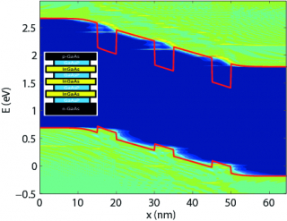
Nanostructures such as quantum wells, nanowires, or quantum dots are attracting a lot of attention as the active components of photovoltaic devices due to their improved energy conversion efficiency. To design them, it is important to precisely know where their conduction and valence band edges lie and how the resulting light absorption spectrum looks like. At the Integrated Systems Laboratory, we have recently developed a device simulator that allows one to construct nanostructures atom by atom and accurately calculate their optical properties. Presently, this modeling tool assumes that electrons and holes are captured within the simulation domain and cannot escape it. However, in reality, a current flows through the considered nanostructures, thus impacting the distribution of the electron and hole population. The goal of this project is to extend the existing simulation approach so that current flows can be taken into account in the calculation of the optical properties of solar cells.
Status: Available
- Looking for 1..2 Semester/Master student(s)
- Contact: Mathieu Luisier
Prerequisites
- Interest in device physics
- Flair for computational modeling
- Experience with Matlab and/or C/C++ programming
Character
- 40% Theory
- 40% Implementation
- 20% Testing
