FPGA mapping of RPC DRAM
From iis-projects
Contents
Overview
Status: Available
- Type: Bachelor or Semester Thesis
- Professor: Prof. Dr. L. Benini
- Supervisors:
Introduction
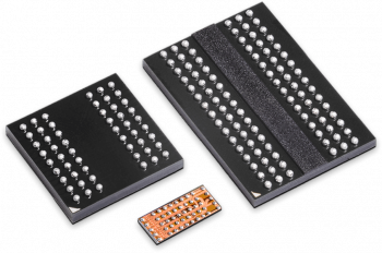
Recently, a new class of off-chip memories hit the market, targeting low area and low pin-count FPGAs and ASICs. These reduced pin count DDR (RPC DDR) [1] memories only require a simple on-chip PHY and can operate with regular digital IO pads making them usable on our ASICs.
In previous projects, we implemented a memory-controller for RPC DRAM and taped it out on two different chips [2][3]. While their testing is ongoing, a readily available FPGA map is useful for fast prototyping and assessment of the IP.
Project
The goal of the project is to map the RPC memory controller on FPGA and verify its functionality according to specifications. Functionality is verified by means of:
- Cycle accurate RTL simulations using a model of the RPC DRAM endpoint provided by the DRAM manufacturer
- A custom PCB with standard FMC termination that can be plugged into a FPGA board. The target board is Digilent Genesys II.
Both 1. and 2. above are started to provide a reference setup to the student.
As a last note, the memory controller is part of Cheshire [1], a platform hosting a linux capable RISC-V 64-bit core. An FPGA flow for mapping Cheshire on a Genesys II FPGA is already available.
The student will:
- Get familiar with RPC DRAM protocol and the controller design
- Implement the design on FPGA: while a 1-to-1 correspondence between ASIC and FPGA exists, some differences may arise at the level of memory buffers and low-level cells (e.g., clock multiplexers), which require a dynamic switch between the two targets due to implementation differences.
- Verify design functionality according to 1. and 2. above, and assess performance (bandwidth, utilization)
Character
- 20% Literature Review
- 60% Hardware Design
- 20% Verification and Bechmarking
Prerequisites
- Strong interest in computer architecture and memory systems
- Experience with digital design in SystemVerilog as taught in VLSI I
- Preferred: Knowledge or experience with AXI and RISC-V
