5G Cellular RF Front-end Design in 22nm CMOS Technology
From iis-projects
Short Description
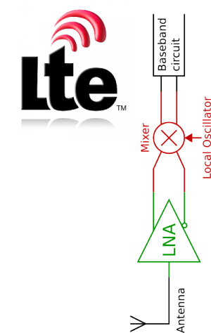
In a transceiver IC, the analog front-end is the first circuit that processes the received signal from the antenna. In modern transceiver ICs (e.g. for LTE application) the front-end amplifies the signal prior to a direct downconversion to baseband. Both the amplification and frequency conversion stage have to show a very low noise figure and have to be free of harmonic distortion. As more and more digital functions are integrated on the transceiver IC, ultra-scaled digital CMOS starts offering big advantages in terms of area and power consumption. Those technologies pose new challenges and offer new opportunities to the analog front-end design. In this work the analog front-end for the up-coming 5G standards will be implemented in a 22nm CMOS technology. Different topologies for the low-noise-amplifier (LNA) and the mixer (frequency translation circuit) shall be analyzed and compared. The most promising will be implemented and verifed in the mentioned IC technology.
Status: Available
- Looking for 1-2 Semester/Master students
- Contact: Thomas Burger
Prerequisites
- Analog Integrated Circuits
- Communication Electronics (recommended)
Character
- 30% Theory
- 60% ASIC Design
- 10% Layout
